P-N Junction
Forward Bias
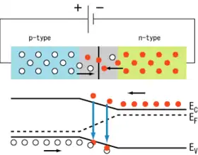
The rectifying action of semiconductor diode is due to the electrical effects that occur at the junction between the n-type semiconductor and p-type semiconductor, at a region known as p-n junction (gray areas in images shown below)
As seen in the images below: If the positive terminal of the power source is connected to the p-type semiconductor and the negative terminal of the power source is connected to the n-type semiconductor, the electron flows across the junction from n-type material to p-type material, and the holes flow in reverse. This will cause the junction area to become narrower allow easy movement of both holes and electrons.
These phenomena are known as forward bias. The p-n junction will be narrower and will allow more electrons to fill into holes and the holes will move to capture electrons.
Reverse Bias
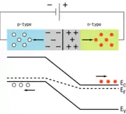
If the power source is installed in reverse, the positive charge in n-type and negative charge in p-type will oppose electron movement causing potential barrier.
The p-n junction will widen, both electrons and holes will be moving away from the junction and causing no current that can flow across the junction. These phenomena are known as reverse bias.
Hence, it acted more or less like a one-way valve for electricity flow.
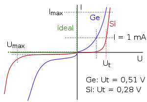
IV curve
The graph shown is a current-voltage characteristic of p-n silicone diode.
From IV curve
- .
- .
- .


Conducting voltage of diode
Conducting voltage of diode represents diode biasing voltage to conduct current . Conducting voltage of diode has a symbol Silicon (Si) diode is 0.7 V Germanium (Ge) diode is 0.3 V
